Barriers of frequency growth
Evgenie Rudometov
authors@rudometov.com
On path of increase in productivity of processors at the expense of reduction of scale of lithograph and growth of clock rates there are the barriers linked to physical laws. Solution of problems – in development and implantation of the newest processing techniques and architectures.
For rather short period of development of the computers created on the basis of semiconducting units, computing power of these become irreplaceable arrangements has increased in many thousand times. It was promoted to no small degree by evolution of the architecture of processors and perfection of their inner patterns. Offered innovations realised by means of the newest solid-state technologies provided constant growth of the clock rates providing increase of productivity.
From the point of view of the user, productivity of the processor is an execution time the certain instruction set which sequence derivates a computer program. The it is less, the better, that is the processor used in system is especially efficient. It means, that it is possible to understand quantity of the commands executable for clock tick as productivity, increased by clock rate of the processor:
Productivity = (Quantity of commands for clock tick) h (Clock rate)
The quantity of the commands executable for clock tick, depends both on the executable program, and from the processor architecture (with what set of computer instructions the processor is capable to work and as this operation is carried out). At processor level one command of the program will be transformed to some machine instructions or elementary commands, and efficiency of such conversion depends and on the processor architecture, and from code optimisation under the concrete architecture of the processor. Besides, depending on the processor architecture elementary commands can be executed in a parallel way.
By the way, from the aforesaid it should be clear, that it would be incorrect to compare productivity of the processors having the various architecture, being grounded only on clock rate of processors. That is why at the same clock rate one applications can be fulfilled on processors, for example, from Intel company, and others — on processors from AMD more effectively .
However if to consider the same set of the processors presented by models of the identical architecture, to compare their productivity, proceeding from clock rate of the processor, it will be quite correct.
So, for rise of productivity of the processor it is expedient to raise clock rate of its operation, is more exact than a semiconducting crystal — kernels of the processor making a basis of this major unit and defining its possibilities.
Each processor is calculated for the specified frequency and if the processor, say, is calculated for operation on frequency of 3 MHz, it not whim of the manufacturer, and an objective reality. Certainly, initially processors of one modelling bar are made on the same processing technique, in the same conditions and on the same contribution link. However on any production, owing to various circumstances, there are deviations from the set norms which lead to that chips of processors have a little excellent from each other characteristics. For revealing of consequences of such deviations the technical control and production testing are carried out. Certainly, to test separately each chip at all numerous stages of its manufacture, considering scales of similar production, it is not obviously possible. The poet, as a rule, holds selective testing from each party of finished goods. During testing ability of processors to work on this or that frequency then all party of processors is labelled according to the given frequency comes to light. There is a probability of that the processor gained by the user has not transited selective testing and is capable to support a little big frequency, than is specified on marking. Besides, the manufacturer pawns some "degree of safety" considering statistical dispersion of parametres, linked to impossibility to provide 100 % of repeatability of productions. As a result the majority of the processors which are coming into the hands of users, can successfully work on the raised frequencies. However recognising possibility of supernumerary modes, it is necessary to consider, that similar modes reduce cannot be recommended for the corporate market linked.
However it is necessary to mark, that in process of perfection of processing techniques with which usage processors are released, the statistical dispersion of parametres is narrowed down. It allows not only to reduce "degree of safety" installed by the manufacturer, but also step-by-step to release within the limits of technological possibilities more and more efficient models. However step-by-step the processing technique spare is settled. And despite perfection of internal design of a kernel, release of new models of the upper frequency range all is given more difficultly and more difficultly.
And still, what stirs to borderless growth of frequency of operation of inner patterns of a semiconducting kernel of the processor, what effects, what physical processes interfere with this process?
To answer this question, it is necessary to remind, that modern processors of desktop computers already rather consist for a long time of tens millions units. These units are presented by the field-effect transisors made on special processing technique of CMOS (the complementary logic on the basis of processing technique metal-oxide-semiconductor, CMOS). Moreover, the semiconducting kernel Northwood created on processing technique of 130 nanometers and long time were basis of processors of Intel of Pentium 4, incorporates 55 million transistors. However 90 nanometers promptly replacing the predecessor have received kernel Prescott on some tens millions units more therefore the number of transistors has reached astronomical value in 125 million
Here it is necessary to remind, that parametres of transistors substantially depend on their standard sizes. Change of standard sizes is defined by evolution of a procedure according to which release of processors is carried out. Key parametre characterising tehprotsess, the scale of processing technique defining the sizes of semiconducting units, internal chains of the processors consisting from in appropriate way of transistors jointed among themselves making a basis is.
Table 1. Evolution of a procedure of the corporation of Intel
The process name |
P854 |
P856 |
P858 |
Px60 |
P1262 |
P1264 |
P1266 |
P1268 |
Implantation, year |
1995 |
1997 |
1999 |
2001 |
2003 |
2005 |
2007 |
2009 |
Scale, nanometer |
350 |
250 |
180 |
130 |
90 |
65 |
45 |
32 |
Slice Si, mm |
200 |
200 |
200 |
200/300 |
300 |
300 |
300 |
300 |
Interconnectings |
Al |
Al |
Al |
Cu |
Cu |
Cu |
Cu |
Cu |
Length of a lock, nanometer |
350 |
200 |
130 |
70 |
50 |
30 |
20 |
15 |
Gate dielectric |
SiO2 |
SiO2 |
SiO2 |
SiO2 |
SiO2 |
SiO2 |
High-k |
High-k |
The channel |
Si |
Si |
Si |
Si |
Strained Si |
Strained Si |
Strained Si |
Strained Si |
Improvement of processing technique and proportional reduction of the sizes of transistors promote improvement of their parametres, major of which are their high-speed properties.
At reduction of length of a lock () in M of times in the proportional image frequency parametres and density of allocation of transistors increase.
Table 2. Change of parametres of transistors depending on their standard sizes
Parametres |
Koffitsient |
Length of a lock (X) |
1/M |
Lock width (Y) |
1/M |
Thickness of a lock (Z) |
1/M |
Allocation density |
M*M |
Frequency of operation |
M |
Power |
1/M |
The sizes of each of the transistors which are a part of processor kernel Prescott, already it is less all than a known virus of a flu. Jointed definitely among themselves more than hundred millions microscopic transistors are concentrated to extremely small square and work quite often on the frequencies, considerably exceeding ten gigacycle. It is obvious, that all these units make against each other mutual negative impact. It is possible to illustrate this influence easily on an example of two nearby explorers jointing units in a kernel of the processor.
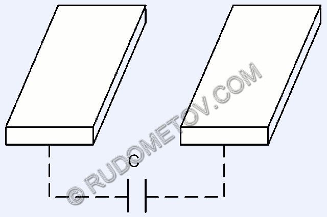
Fig. 1. Two nearby explorers, jointing units in a kernel
These explorers possess mutual capacitance. This size, as is known, depends on distance between explorers and squares of the sides paid to each other under the known formula: C = k ґ S / d where With — size, S — square, d — distance, k — the coefficient, which sense will be specified further.
Because of mutual capacitance uncontrollable currents as on high frequencies the capacitor derivated by explorers possesses conductance though for a direct current such layout is a reliable insulator are derivated. Certainly, estimating behaviour of the resulted circuit on high frequencies, it is necessary to notice, that the sizes of explorers are small, but it is not enough and distance between them. Considering values of frequencies, and also quantity of such explorers which number makes many millions, it is possible to assert, that their influence on frequency properties of inner patterns of a processor kernel cannot be neglected. Especially if to take into consideration that circumstance, that each explorer possesses also ohmic resistance, and inductivity. And it means, that the equivalent circuit of two explorers represents a collection of sizes, resistors and induktivnostej. It is obvious, that it possesses properties of the integrating circuit with numerous resonances. Moreover, in a real life it is necessary to consider cross-coupling of several explorers against each other. It illustrates the following figure on which the variant of three explorers is presented.
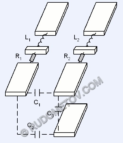
Fig. 2. A variant of three nearby explorers jointing units in a kernel
Possibly, there is no necessity to prove, that frequency properties of such system it is already much more difficult than a simple variant of two explorers. It is necessary to add, as active (resistances), and wattless (sizes, inductivity) components of a complete impedance are distributed on all length of explorers. It is multiple complicates the description and behaviour of similar systems on high frequencies. However the situation becomes even more difficult if to recollect, that the described system is not in vacuo, and between explorers there are the substances possessing in certain dielectric parametres, influencing values of mutual capacitance. Moreover, considering, that the dielectric coefficient of substances used in chips is more than unit, mutual capacitance values in comparison with the previous cases increase in appropriate way. The approximate circuit is resulted on fig. 3.
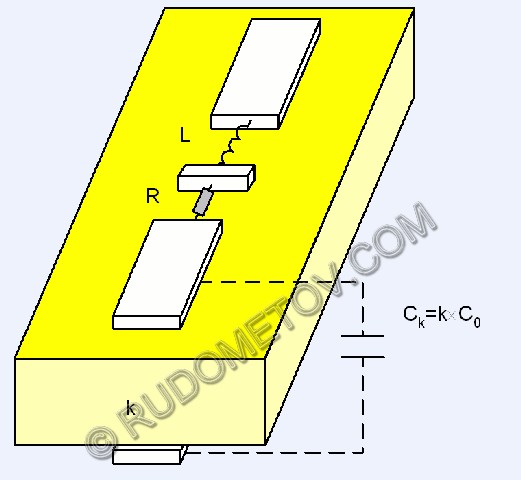
Fig. 3. The variant of two explorers considering influence of dielectric materials
From the resulted figure it should be clear, why designers aspire to use for a device isolation of monolithic microcircuits substances with the smaller value of a dielectric coefficient (k).
It is necessary to add, that high-frequency parametres of the described circuits depend on many factors. It is enough to enumerate, for example, the geometrical sizes of explorers, their relative positioning, structure of metals and environing dielectric materials, microscopic defects. Any variations of these parametres generate respective alterations in frequency properties. By the way, it is one of the necessity reasons to pawn "degree of safety" in difficult high-frequency products.
Except topology of explorers it is necessary to consider and influence of transistors, whose structure and a physical essence is much more difficult than separate explorers, at least because they are active components. However transistors not only exercise administration of electrocurrents flowing through them, fulfilling functions of high-speed electronic keys. The matter is that these miniature semiconducting units are powerful sources of electromagnetic emanation. Thus, having electromagnetic effect on adjacent units, they in turn test similar influence from adjacent chains. Entering into structure of transistors p‑n‑переходы are capable to carry out unforeseen detecting of the induced currents, their strengthening and the subsequent transmission. By the way, it is difficult to present and precisely to describe an electromagnetic background in chips of processors which thanks to close packing of units is characterised by variation fields very much a high tension. This field derivates difficult structure which continuously varies according to different frequencies of operation of inner patterns of the processor, variable maxima and minima in different sites of a semiconducting crystal of the processor which picture permanently varies according to executable operations are thus derivated.
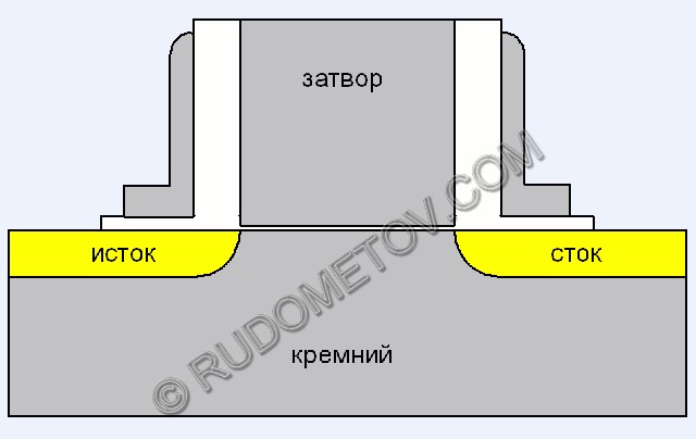
Fig. 4. Structure of traditional CMOS-transistor
The overall picture is multiple becomes complicated if to consider, that the sizes of transistors have already reached those values when quantum effects start to render the increasing influence. The given effects, despite constant perfection of the architecture of transistors and reduction of their sizes, promote increase in uncontrollable currents. Their common stream is added from the currents generated neidealnostju of isolation, and also leakage flow of the various nature through interelement sizes and even at the expense of Esaki effect.
Result of miniaturization of the semiconducting units making a basis of electronic circuits on semiconducting silicon chips and working on hyperfrequencies in the conditions of considerable electromagnetic interferences, prompt growth of a leakage current is.
Here it is necessary to remind, that for saving of stability of operation of electronic circuits, the currents inspected by working units, should be more than an uncontrollable leakage current. As a result of the negative phenomena generated by processes of miniaturization, the uncontrollable currents which basis is made by a leakage current, and also the stray currents linked to growth of frequency of switching of transistors, limit reduction teploobrazovanija processors. It means, that expected essential reduction teploobrazovanija does not occur, despite the reduction of a supply voltage reached thanks to reduction of standard sizes of transistors.
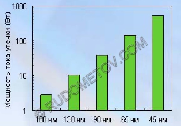
Fig. 5. Growth of power of a leakage current because of reduction of standard sizes of transistors CMOS (on substances IDF)
The share of the specified uncontrollable part of a current flow considerable enough also increases with frequency growth. It is one more reason forcing the manufacturer to pawn in the semiconducting products "degree of safety".
In struggle against growth of the negative tendencies occurring in electronic circuits, the processors realised in chips and other chips, experts insert new processing techniques. As an example it is possible to result, for example, usage of copper explorers instead of aluminium, substances with low metrics of a dielectric coefficient - low k, processing techniques of intense silicon - Strained Si and silicon-on-insulator – SOI.
Changeover of aluminium by copper for explorers jointing transistors has provided lowering of losses at signal transmission. As a result it has reduced as a whole a heat release and has allowed to increase clock rates of the processor.
The same purposes were pursued by implementators, applying substances low k and Strained Si. The first, used for isolation of internal chains, including jointing explorers, reduce values of the parasitic interelement sizes interfering growth of clock rates. The second are intended for reduction of a channel resistance a source-drain. It is linked by that intense silicon, is characterised by the big distance between atoms of its space lattice that provides a smaller resistance to electron flow. And it reduces a heat release and allows to increase clock rates.
It is necessary to mark, that usage and such processing techniques, as SOI is routed struggle against a heat release. This processing technique provides lowering of stray currents through a wafer.
The similar purpose, but only for chains of locks, application of substances with high k is routed also . These substances it is planned to use as insulating layers of locks of transistors of in exchange traditionally applied film of silicon oxide. A thickness of this film already makes less than ten atoms that calls a considerable uncontrollable leakage current. Usage of new substances will allow to reduce a leakage current approximately in one thousand times. It considerably will reduce a heat release and will allow to increase clock rates. To the same purpose in addition to usage of substances high k there will be a changeover polikrastallicheskih locks on the metal. Further it is necessary to expect application so-called trehzatvornyh structures and teragertsevyh transistors.
Implantation of the specified innovations will allow to continue process of miniaturization of units, increasing their frequency potential and density of allocation of transistors on semiconducting crystals. The last parametre allows to increase from generation to generation quantity of the transistors which are the centre of the processor. The given array is a resource of implementators and accordingly a source of increase in potential possibilities computer completing, and consequently and created products.
Growth of the array of transistors occurs according to Moore's empirical law according to which prompt evolution of chips and perfection of the architecture of processors is carried out. Result is growth of clock rates and increase in productivity of processors.
For compensation of the negative phenomena and support of a quiescent operation of processors on high clock rates manufacturers should increase a supply voltage of kernels. It is possible to be convinced of justice of this statement if to compare levels of regular supply voltages for low and high models of processors. Irrespective of processing technique and the architecture of processors for high models of one bar a kernel supply voltage, and also power teploobrazovanija always above. However such increase, as a rule, does not carry on to essential abbreviation of periods of operation of processors at the expense of the accelerated degradation of semiconductors.
It is necessary to mark, that thermal power tends the last years growth even in regular modes of processors. And it in spite of the fact that designers in struggle for its lowering perfect inner patterns of processors and try to reduce power kernel power supply. By the way, lowering of levels of power supply became possible thanks to reduction of the geometrical sizes of transistors, and, as consequence, reduction of the sizes of their locks. Really, the Source-drain (Source-Drain) controls a current the lock field (Gate), and the the lock is more thin, the the smaller power is required on a lock for saving of demanded field intensity.
In addition to it, channel length abbreviation is accompanied by reduction of losses, including dzhoulevo warmly. Besides, to improvement of parametres promote as well the newest developments in the field of topology of transistors.
Perfection of the architecture of processors and procedure of their production provides growth of clock rates and computational capability of processors (fig. 6).
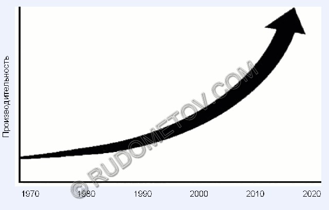
Fig. 6. Exponential growth of productivity of processors (on substances IDF)
Unfortunately, an underside of this growth, besides, is rather fast increase teploobrazovanija processors. Considering that fact, that the square of a chip of the processor practically remains to a constant, growth teploobrazovanija promotes increase in density of energy.
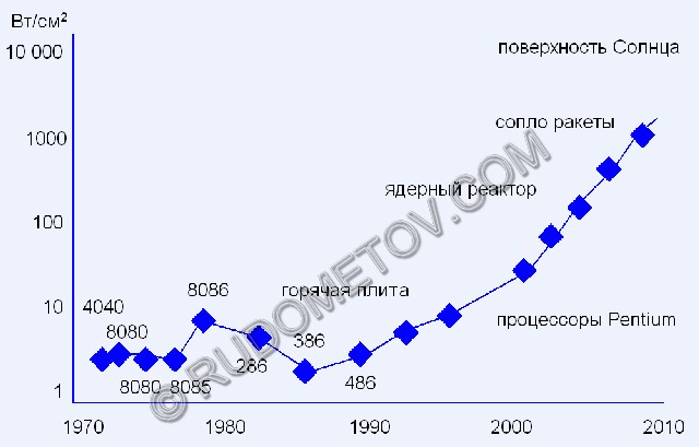
Fig. 7. Growth of density of energy in a chip of the processor and its comparison to other systems (on substances IDF)
High power teploobrazovanija in case of inadequate resources of cooling is accompanied by an overheat of inner patterns of the processor, that negatively affects working capacity, and also strengthens and reproaches processes of degradation of semiconductors.
Really, from physics it is known, that semiconductors are extremely sensitive to temperature increase. At rise in temperature average energy of oscillation of atoms grows in a chip. As a result the increasing quantity of links in silicon space lattice starts to be broken off, there are all new steams elektronov and holes. Starting from the certain moment of growth of temperature, semiconductor properties vary, for example, with growth of temperature conductance of semiconductors and dielectric materials increases. As result, there are glitches and repeating lags. Struggle against these effects necessity for usage of adequate resources of maintenance of optimal temperature modes speaks. Already any high-frequency, high-powered processor does not do without appropriate coolers in which structure massive heat sinks and powerful cooling fans are applied. It is logical to assume, that, having taken special measures on processor cooling, it is possible to achieve a stable operation of the chips calculated for a room temperature, — and on the clock rates considerably exceeding "regular" megacycles. Not advertised measures similar, as a rule, widely, were applied, in particular, at demonstratings at Forum IDF. During these actions possibilities of the perspective processing techniques underlying high-powered processors were shown.
Coming back to a question high teploobrazovanija, it is necessary to mark, that, unfortunately, supply voltage and clock rate rise increases thermal power. And it as it was marked above, is accompanied by a number of the negative phenomena among which it is possible to result and local, and the common overheats of a semiconducting crystal with all negative consequences following from this fact. Besides, it is impossible to dump about scores and the raised levels energopotreblenija, heavy burden of computer systems laying down on electric power supplies, and necessity of usage of powerful tools of cooling, etc ., etc .
Troubleshooting lowerings energopotreblenija the products, designers began to build in the special chains regulating operation of processors structure of the architecture of kernels. The given chains, whose functioning it is supported by the system software, depending on computing load and conditions of service provide installation of optimal electrical and frequency modes. It, in particular, means, that in case of lowering of computing load there is a reduction of clock rate of operation of a kernel.
By the way, at lowering of clock rate of the processor below the regular value, the supply voltage of its kernel can be lowered in appropriate way without violation of stability of system operation. It allows teploobrazovanie the processor. Such operations executable in an automode by a firmware, are standard for laptops and are intended for saving of energy of batteries. However power and frequency lowering already uses and for models of server sector of the computer market. By way of illustration it is necessary to mention realised in recently released on 90 nanometer tehprotsessu models of Intel Xeon (kernel Nocona) processing techniques Demand Based Switching (DBS) and Enhanced Intel SpeedStep – dynamic regulation and a processor power reduction.
For an estimation of efficiency of similar processing techniques for lowering of thermal load on a processor kernel it is expedient to take advantage of the following formula:
P »CЧV2ЧF
Where P — thermal power of the processor, With — the coefficient considering mutual capacitance of units of a kernel of the processor and depending on the architecture of its kernel (usually increases with increase in density of chip planning of a chip), V — a kernel supply voltage, F — clock rate.
The given formula it is possible to lead to sort:
 Where variables with an index k designate appropriate parametres of changeable modes, and variables with a zero index — parametres of a regular mode.
Using the resulted formula, it is possible to notice, that reduction of clock rate and a kernel supply voltage by 5 % provides power lowering teploobrazovanija almost on 15 %. Reduction of clock rate by 10 %, and supply voltages by 7 %, leads to lowering energopotreblenija, and, therefore, and teploobrazovanija almost on a quarter.
It is necessary to add, that the extension of frequency and energetic control bands leads still bolshemu to level reduction teploobrazovanija. And it reduces thermal load on a semiconducting crystal of the processor and a cooling resource, electrical – on units energopitanija even more. Besides, thanks to reduction of temperature in tank conditions of service of other components of system improve.
By the way, in transportable systems such approach allows to reduce energopotreblenie several times.
In summary, it is necessary to mark, that, despite existing barriers on path of rise of productivity of units and sitem, scientists and engineers successfully overcome them. They offer various paths of solution of problems rising before computer branch. It and improvement semiconducting tehprotsessov, and perfection of the architecture of high-frequency chips, and implantation of perspective processing techniques, and even retrieval of paths of modification konstruktivov system units.
As an example it is possible to name, for example, Sun, DEC, IBM, Compaq. By the way, in 1991 started the joint project of Intel and NCR on “industrial temperature dispersal”, known under name Cheetah. The briefcase of the patents registered within the limits of the project, has passed in the instruction of six founders of KryoTech corporation which at that time were engineers NCR later. Further the given developments have allowed experts of KryoTech corporation to create the whole series of the installations providing effective cooling of server processors, maintained in the forced modes at the expense of their premise together with motherboards in freezing cameras. However this subject already other articles.
Article is published in log Byte (http://www.bytemag.ru).
 English
 Russian
 German