 English
 Russian
 German
The computer equipment future
(Continuation)
Evgenie Rudometov
Victor Rudometov
authors@rudometov.com
Engineers have already faced it and many other things negative effects at transition to processing technique of 90 nanometers. Really, in the new products created on this processing technique, the small use in the world CMOS transistors (CMOS) with length of a lock 50 nanometers, including the contribution of Esaki effect,
Experts all over the world persistently search for paths of overcoming of the negative effects interfering further perfection of the architecture and growth of productivity of processors.
One of perspective methods is linked to usage of so-called intense silicon (Strained Silicon). The essence consists in silicon doping by small additives of germanium. As a result the distance between atoms in silicon space lattice increases, that is the lattice is as though expanded, as has given processing techniques the specified name. As the result of such impurity-dopant incorporation decreases a channel resistance the Source-drain to the electron flow providing a current flow. And it is accompanied by reduction teploobrazovanija.
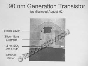
Besides, implantation of processing technique of silicon on an insulator (silicon on isolator — SOI) allows to reduce considerably a leakage current, at the expense of separation of the channel the Source-drain from a wafer.
All it allows to increase frequency, and, therefore, and productivity of operation of chips.
Basis of the future models will make so-called teragertsevye transistors. In the performance Patrick Gelsinger: “We consider this transistor as absolutely new fundamental architecture. And we will expand this direction in the following of 10 years and further”.
Here it is necessary to remind, that high operating frequencies of modern chips are provided with appropriate characteristics of units entering into their structure. Considering complexity of the inner patterns consisting of hundreds of transistors, and also their synchronisation it is necessary to use rather high-frequency units. Thus their frequency range should be 10 times wider, at least. And it means, that in case of processors of Intel of Pentium 4, ALU which work on the doubled clock rate, the architecture demands already today the units which frequency potential makes tens, and in any situations, maybe, and hundreds gigacycles.
And all it concerns not only servers, powerful workstations, but also mass desktop computers and even portable solutions.
By the way, having mentioned sector of transportable computers it is necessary to mention processors of absolutely new architecture. It is a question of the processors which basis is made by the architecture of the kernel which have received name Banias. This processor already named as Intel Centrino, consists approximately of 77 million transistors. It provides not only considerable growth of productivity of transportable computers, but also raised time of their operation from the built in secondary generators. Thus for reaching bolshej electric power saving, and also a smaller heat release processors can reduce the frequency. In addition to it when processors do not use, they can pass in a sleeping mode. And though clock rates of these processors will be below transportable variants of popular Intel of Pentium 4 with its hyperpipeline, it does not mean its smaller productivity. Besides, there is an underplate to consider, that internal units of a kernel will be, as well as their clones in the previous models of processors, will work on enough high frequencies.
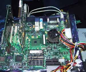
Desktop system with experimental sample Banias
Certainly, high frequencies of the future products will demand new konstruktivov for processors and tanks of system units. But also the processing technique on which the future high-powered units will be made, demands appropriate development. With that end in view experts of Intel have made some fundamental reachings in the field of lithograph. It is a question of program EUVL — Extreme Ultraviolet Lithography, linked to usage of hard ultra-violet radiation.
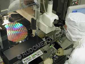
Experiment with processing technique of 90 nanometers
Mass production of chips on this processing technique is planned on second half of current decade, but in connection with a rapid progress in this area probably and earlier. Thus Patrick Gelsinger considers, that the given perspective processing technique will be used even after the lapse of 2010.
The specified processing technique will allow to release very difficult products with the big number of the transistors working on very high frequencies and allocated on semiconducting crystals of critical dimensions.
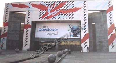
Developer forum hardware and the software in San Jose
However high density of the active components allocated on silicon chips, generates a problem of high density of energy of the heat release already today exceeding level of a hot plate, and the next years will reach and even will exceed level of density of energy of a nuclear reactor. It very much high levels, but for experts are not present doubts, that all problems arising in engineering process of new products, will be successfully solved.
Continuation follows
In article substances IDF, and also open documents have been used
Intel corporations.
It is published in log "the Express train Electronics"
To pass to razrelu Processors