 English
 Russian
 German
The first products of processing technique of 90 nanometers
Evgenie Rudometov, Victor Rudometov.
authors@rudometov.com
Article is grounded on substances of books "Arrangement of the multimedia computer" and "Motherboards and chip sets"
Each two years in the computer industry change of a procedure is carried out. In spite of the fact that process 0,13 microns is inserted yet by all main manufacturers, a number of corporations declare the operations linked to mastering of processing technique of 0,09 microns.
Has transited already over three tens years after appearance of the first microprocessor. Every year these units all become more difficult. Thus the number of the transistors making their basis and defining computing power, increases on an exponential low. This growth is well described Moore's predicting regular doubling of number of transistors in computer components by the known law.
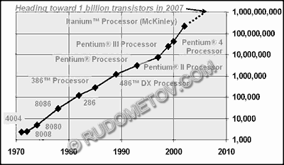
Fig. 1. Growth of number of transistors in processors
The increase in functionality of computer components, including growth of their power, substantially depends on their architectures which implementation is defined by the reached level of processing techniques.
Development of the electron technologies, aspiring to operate with more and more miniature units, allows to increase all time their number, providing designers possibility to complicate the architecture of created products.
Thus it is necessary to understand, that each reached technological level has the limit limiting number of elementary transistors. Really, growth of the sizes of chips carries on to growth of their price, and the density increase is limited both the sizes of units, and problems teploobrazovanija.
All aforesaid concerns all products, but especially strongly appears for processors of computers.
It is necessary to mark, that approximation to a technological limit leads to a low dice yield and, accordingly, to growth of the cost price for high models. In process of growth of computational capability of processors, them energopotreblenija and, as consequence, increases teploobrazovanija, become aggravated problems of maintenance of optimal temperature modes their operations reaching of critical values near to technological limits. All it constrains further development of the architecture of processors and growth of their power.
In spite of the fact that the procedure 0,13 microns is mastered far not by all corporations occupying the upper lines of ratings, the industry actively prepares already for the next boundaries. Following such stage is the processing technique 0,09 microns (90 nanometers).
Here it is necessary to remind, that on this path there are many problems.
It is obvious, that with reduction of distances between units and interconnectings in chips of processors level of electromagnetic interferences increases, a leakage current increases, thermal load on sites and the separate units making a basis of kernels grows. Thus it is necessary to mark, that the sizes with which implementators operate, fast come nearer to those thresholds where the quantum effects complicating processes of engineering more and more affect, production and maintenance.
Nevertheless, problems and the difficulties arising before designers, do not stop engineering thought. As a result there are new processing techniques and perspective products.
Contributors of corporation of Intel have created the smallest in the world storage location of standard SRAM (Static Random Access Memory — a static random-access memory). The square of this storage location makes only 1 square micron.
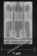
Fig. 2. The smallest in the world storage location of standard SRAM
Each such mesh represents a structural component of a chip of memory and is a part of a full-function chip of memory SRAM in size of 52 Mbit.
The created chips are among most capacious of ever created chips of memory of standard SRAM, in each of which contains on 330 million the transistors allocated on square of 109 square millimetres.
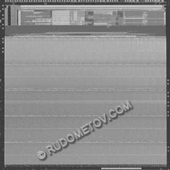
Fig. 3. A chip of most capacious of ever created chips of memory of standard SRAM
By the way, the square of a chip of the created chip of memory is less, than, for example, for desjatitsentovoj coins.
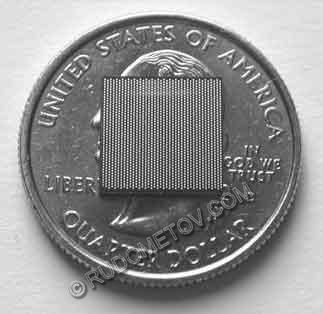
Fig. 4. A chip of a chip of memory SRAM
New 52-megabit chips of memory of standard SRAM have been created at experimental factory D1C of corporation of Intel on output on 300-cross-section wafers in Hillsboro, the State of Oregon, with usage of a combination of the advanced lithographic tools of 193 and 248 nanometers on developed by experts of Intel 90-nanometrovoj processing techniques.
It is necessary to mark, that production of chips of memory of standard SRAM traditionally uses in branch for testing of new processing techniques. Thus the storage location mesh size plays exclusively important role. The matter is that similar units use as a part of processors as a part of the cache memory of processors.
Thus, advanced design of engineers of Intel will allow to increase productivity of the processors.
The given development is the important step on path of mass implantation of new industrial processing technique in 2003, intended already in the near future to replace the predecessors — processing techniques 0,18 and 0,13 microns.
Evolution of a procedure
|
The process name |
P854 |
P856 |
P858 |
Px60 |
P1262 |
P1264 |
|
Implantation, year |
1995 |
1997 |
1999 |
2001 |
2003 |
2005 |
|
Lithograph, nanometer |
350 |
250 |
180 |
130 |
90 |
65 |
|
Length of a lock, nanometer |
350 |
200 |
130 |
<70 |
<50 |
<35 |
It is necessary to remind, that Intel corporation namerena to insert 90-nanometrovuju processing technique in mass production within next year, thereby once again in practice having confirmed 12 years operating already the law on transition to the new generation "know-how" each two years. On new processing technique the corporation will make the majority of production, including processors, chipsets and the communication equipment. Production on the given processing technique will be made exclusively on 300-cross-section wafers, operation with which is mastered in the course of mastering of the previous process 0,13 microns (130 nanometers).
Processors Prescott declared on IDF Spring 2002 become the first products released on processing technique of 90 nanometers. Predictably, chips Prescott can evolve to clock rates of 5-6 GHz. The Japanese sources seriously discuss possibilities of appearance and usage of variant Mobile Prescott. It is linked with expected low enough energopotrebleniem the processors created on processing technique of 90 nanometers.
However, describing reachings of experts of Intel, for the sake of justice it is necessary to mark, that schedules of the accelerated implantation of perspective processes have declared also other large firms.
The companies of IBM Corp., Toshiba Corp., Sony Corp. And Sony Computer Entertainment Inc. Have declared the beginning of joint development tehprotsessov 90 nanometers and 45 nanometers. For it the companies namereny to spend "some honeycombs millions dollars". And, in spite of the fact that on available earlier given UMC was gathered to start mass release 0,13 microns only in the summer, on the Internet there were messages on schedules of this corporation to start release by the end of year of the chips created on processing technique of 90 nanometers.
Most likely 2002 will be roast.
In article substances IDF Spring 2002 and documents of the corporation of Intel have been used
Article is published in log "Computer-price"
To pass to razrelu Motherboards and chip sets