 English
 Russian
 German
Spring 2002: from 130 nanometers to 90 nanometers
Evgenie Rudometov, Victor Rudometov.
authors@rudometov.com
Growth of functionality and power of computer accessories is impossible without perfection of processing technique of their production. Therefore each two years in the computer industry change of a procedure is carried out. In spite of the fact that process 0,13 microns is inserted far yet by all manufacturers, leaders of the computer market carry on the intensive researches linked to mastering of processing technique of 0,09 microns.
Has transited already over three tens years after appearance of the first microprocessor which has begun appearance of compact and reliable computers, functionality and which computing power permanently increases with the advent of new models of processors. In the course of continuous perfection these extremely important accessories every year all become more difficult. The number of the transistors making their basis, increases on an exponential low. This growth is well described Moore's predicting regular doubling of number of transistors in computer components of each 1,5-2 years by the known law.

Fig. 1. Gordon Moore (Gordon Moore, Chairman Emeritus of Intel Corporation)

Fig. 2. Growth of number of transistors in processors
The increase in functionality of computer components, including growth of their power, substantially depends on their architectures which implementation in appropriate chips of chips is defined by the reached level of processing techniques.
Development of the electron technologies, aspiring to operate with more and more miniature units, allows to increase all time their number. It provides to designers possibility to complicate the architecture of created products and to expand a band of functions.
However it is necessary to understand, that each reached technological level has the limit limiting number of elementary transistors, chips allocated on chips.
Really, growth of the sizes of chips carries on to growth of their price. First of all it is linked to reduction of an output of finished articles from one slice. Here pertinently to remind, that chips of chips of the future products form simultaneously in the course of multiphasic processing of a slice. Besides, it is necessary to add, that with growth of square of chips the probability of appearance of defects increases.
The density increase is limited both the sizes of microcomponent parts, and a number of the problems following from laws physicists of semiconductors and features of engineering of modern high-frequency electronic circuits.
All aforesaid concerns all products, but especially strongly appears for such difficult and important accessories, as processors of computers.
It is necessary to mark, that approximation to a technological limit leads to a low dice yield and, accordingly, to growth of the cost price for high models. In process of growth of computational capability of processors, them energopotreblenija and, as consequence, increases teploobrazovanija, become aggravated problems of maintenance of optimal temperature modes their operations reaching of critical values near to technological limits. All it constrains further development of the architecture of processors and growth of their power.
Designers should solve the specified uneasy tasks permanently. So there were and with processes 0, 25 microns, and about 0,18 microns, and about 0,13 microns.
The combination of 0,13-micron processing technique and 300-cross-section wafers allows to increase quantity of processors counting on one wafer almost four times, in comparison with 0,18-micron processing technique on 200-cross-section wafers of the previous generation. By the way, the first in branch has passed to wafers bolshego the size and Intel corporation has reduced the sizes of transistors and connective explorers. As a result of it she has managed considerably to lower the cost price and to lift productivity of processors.
In spite of the fact that the procedure 0,13 microns is mastered far not by all corporations occupying the upper lines of ratings, the industry actively prepares already for the next boundaries. Following such stage is the processing technique 0,09 microns (90 nanometers).
Here it is necessary to remind, that on this path there are many problems.
It is obvious, that with reduction of distances between units and interconnectings in chips of processors level of electromagnetic interferences increases, a leakage current increases, thermal load on sites and the separate units making a basis of kernels of processors grows. Thus it is necessary to mark, that the sizes with which implementators operate, fast come nearer to those thresholds where the quantum effects complicating processes of engineering more and more affect, production and maintenance. The matter is that with reduction of the physical sizes of the units integrated into structure of chips of processors, laws according to which the behaviour of charges is defined, keep away from the classical description more and more. It is enough to recollect, for example, Esaki effect and to present its influence on operation of the future compact, multiple-unit, high-frequency products.
Nevertheless, despite of everything, permanently arising problems and difficulties do not stop engineering thought. As a result of intensive researches there are new processing techniques and products.
As a result of perfection of a procedure of production of semiconductor chips contributors of corporation of Intel have created the smallest in the world storage location of standard SRAM (Static Random Access Memory — a static random-access memory). The square of this storage location makes only 1 square micron.
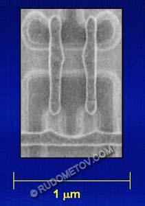
Fig. 3. The smallest in the world storage location of standard SRAM
Each such mesh represents a structural component of a chip of memory. In the course of operations it was possible to reach sizes SRAM of 52 Mbit.
The created chips are among most capacious of ever created chips of memory of standard SRAM, in each of which contains on 330 million the transistors allocated on square of 109 square millimetres.
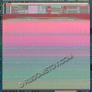
Fig. 4. A chip of most capacious of ever created chips of memory of standard SRAM
By the way, the square of a chip of the created chip of memory is less, than, for example, for desjatitsentovoj coins. Its sizes well illustrates a photo on which this chip is represented laying on dvadtsatipjatitsentovoj to a coin of the USA.
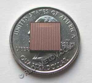
Fig. 5. A chip of a chip of memory SRAM on dvadtsatipjatitsentovoj to a coin
To pass to razrelu Processors