 English
 Russian
 German
Spring 2002: from 130 nanometers to 90 nanometers
(Continuation)
Evgenie Rudometov, Victor Rudometov.
authors@rudometov.com
New 52-megabit chips of memory of standard SRAM have been created at experimental factory D1C of corporation of Intel on output on 300-cross-section wafers (wafer) in Hillsboro, the State of Oregon, with usage of a combination of the advanced lithographic tools of 193 and 248 nanometers on developed by experts of Intel 90-nanometrovoj processing techniques.
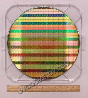
Fig. 6. A 300-cross-section wafer
It is necessary to mark, that production of chips of memory of standard SRAM traditionally uses in branch for testing of new processing techniques. Thus the storage location mesh size plays exclusively important role. The matter is that similar units use in processors as a part of cache memory units.
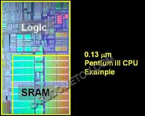
Fig. 7. A chip of the processor of Pentium III, 0,13 microns created on processing technique
Thus, advanced design of engineers of Intel pawns bases on further increase in productivity of their processors.
Development vysokointegrirovannoj chips of memory SDRAM of high size is the important step on path of mass implantation of new industrial processing technique which is intended, to replace the predecessors — processing techniques 0,18 and 0,13 microns.
By the way, experts of Intel namereny and further to reduce low level cells of memory SDRAM, periodically perfecting a procedure.
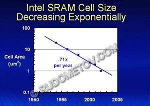
Fig. 8. Mesh sizes in chips of memory SRAM during the period with 1990 on 2005 g
It is necessary to remind, that Intel corporation namerena to insert 90-nanometrovuju processing technique in mass production within next year. Thereby once again in practice having confirmed 10 years operating already more a rule (it installed) to pass to the new generation "know-how" each two years.
Evolution of a procedure
|
The process name |
P854 |
P856 |
P858 |
Px60 |
P1262 |
P1264 |
|
Implantation, year |
1995 |
1997 |
1999 |
2001 |
2003 |
2005 |
|
Lithograph, nanometer |
350 |
250 |
180 |
130 |
90 |
65 |
|
Length of a lock, nanometer |
350 |
200 |
130 |
<70 |
<50 |
<35 |
According to mastering of a new procedure the geometry of transistors will vary also, that visually shows a slide resulted on IDF Spring 2002.
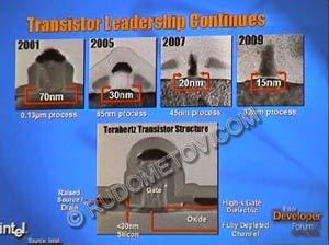
Fig. 9. The transistors created on different processing techniques
New high-frequency, and, therefore, and the efficient processors created on perspective processing techniques, demand appropriate packing of chips of the chips. In this connection on IDF schedules on step-by-step transition on new konstruktivy processors — BBUL have been presented . Difference of it konstruktiva from traditional FCPGA illustrates the resulted photo of a slide with IDF Spring 2002.
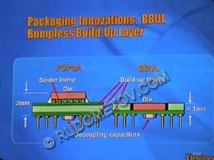
Fig. 10. Processor konstruktivy FCPGA and BBUL
On new 90-nanometrovoj processing techniques Intel corporation will make the majority of production, including processors, chipsets and chips of the communication equipment. Production on the given processing technique will be made exclusively on 300-cross-section wafers, operation with which is mastered in the course of implantation of process of the previous generation — 0,13 microns (130 nanometers).
Models with the code name Prescott, declared on IDF Spring 2002 become the first mass processors released on processing technique of 90 nanometers. Planned to release in 2003 the given bar is the representative of following generation of processors of Intel on the basis of microarchitecture of Intel NetBurst, Pentium used in widespread Intels 4.
By the way, transition to 0,09 microns tehprotsess would allow to reduce kernel Northwood made now on processing technique of 0,13 microns, approximately twice, leaving there is enough place for other architectural improvements.
In processor Prescott, besides other, the processing technique of multithreaded processing of signals Hyper-Threading (this developed Intel the processing technique allows the operating system to work with one processor how if them was two, that considerably raises the common productivity of all platform) will be realised.
Transition to 0,09 microns tehprotsess will allow and to increase further clock rate thanks to what next year it is possible to expect 4 GHz Prescott. Predictably, chips Prescott can evolve to clock rates of 5-6 GHz at appropriate growth of metrics of productivity.
It is necessary to mark, that on the Internet the Japanese sources seriously discuss possibilities of appearance and usage of transportable variants of processors Prescott — Mobile Prescott. It is linked with expected low enough energopotrebleniem the given bar of the processors created on processing technique of 90 nanometers.
On the same processing technique the processors which are successors of existing models of processors, oriented to usage in servers and powerful workstations will be released also. It is a question of processors of IA-64 architecture with code name Montecito. Release of the first models of this processor is planned in 2004 with application of processing technique of 90 nanometers. From characteristics it is necessary to mark the improved architecture at complete program and equipment compatibility with McKinley (0,18 microns) and Madison/Deerfield (0,13 microns).
As Krejg Barrett in the report on IDF Spring 2002 has marked, the next fifteen years development of solid-state technologies will allow implementators of processors to realise following characteristics: 2 billion transistors, clock rate of processors will reach 30 GHz, 1 billion instructions second, the size of transistors — 10 nanometers (0,01 microns), there is possible usage of wafers 18 "(transition with 8" on 12 "slices now is carried out).

Fig. 11. The head of corporation of Intel Krejg Barrett (Craig Barrett, Chief Executive Officer, Intel Corporation)
However, describing reachings of experts of Intel, it is necessary to mark and about schedules of their competitors. A number of large firms was announced by the intentions linked to accelerated implantation of a perspective procedure.
The companies of IBM Corp., Toshiba Corp., Sony Corp. And Sony Computer Entertainment Inc. Have declared the beginning of joint development tehprotsessov 90 nanometers and 45 nanometers. For it the companies namereny to spend "some honeycombs millions dollars". And, in spite of the fact that on available earlier given UMC was gathered to start mass release of chips 0,13 microns only in the summer, on the Internet there were messages on schedules of mastering by this corporation of processing technique of 90 nanometers. Within the limits of led wide area re-structuring, UMC corporation prepares new experts on the Fab 12A which then will work at Singapore factory UMCi of joint venture UMC-Infineon. Approbation of lines on release of the chips created on processing technique of 90 nanometers, is planned by UMC corporation on the third quarter 2002
The specified examples testify to the accelerated implantation of the newest processing techniques in computer branches of the industry which are some years priority directions of development of the leading countries of the world.
At article preconditioning substances IDF Spring 2002, documents of the corporation of Intel, and also the information of some Internet sites have been used.
It is published in log "Terabyte" (N5, 2002)
To pass to razrelu Processors